Journals > > Topics > Integrated Optics
Integrated Optics|39 Article(s)
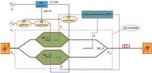
Microring-Based Response-Switchable Microwave Photonic Filter
Liangchen Sun, Jinye Li, Qianqian Jia, Wenqi Yu, Shuangxing Dai, Yiru Zhao, Jiwang Peng, Mingxuan Li, and Jianguo Liu
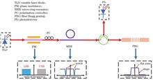
A three-filter-response switchable microwave photonic filters (MPF) based on micro-ring resonator (MRR) and fiber Bragg grating (FBG), using phase-intensity modulation, is proposed and experimentally demonstrated. By tuning the relative wavelengths of FBG reflectance spectrum, MRR notch, and optical carrier, the filter response of MPF can be switched between bandpass, flat-top bandpass, and high-pass. The bandpass, flat-top bandpass, and high-pass responses have bandwidth tuning ranges of 5.56-7.68 GHz, 6.23-11.92 GHz, and 5.83-10.86 GHz, respectively. Insertion loss of MRR under three responses is less than 10 dB. The switchable responses enable the proposed MPF to maintain higher flexibility, with a broad application such as frequency measurement and spurious suppression scenarios. A three-filter-response switchable microwave photonic filters (MPF) based on micro-ring resonator (MRR) and fiber Bragg grating (FBG), using phase-intensity modulation, is proposed and experimentally demonstrated. By tuning the relative wavelengths of FBG reflectance spectrum, MRR notch, and optical carrier, the filter response of MPF can be switched between bandpass, flat-top bandpass, and high-pass. The bandpass, flat-top bandpass, and high-pass responses have bandwidth tuning ranges of 5.56-7.68 GHz, 6.23-11.92 GHz, and 5.83-10.86 GHz, respectively. Insertion loss of MRR under three responses is less than 10 dB. The switchable responses enable the proposed MPF to maintain higher flexibility, with a broad application such as frequency measurement and spurious suppression scenarios.
Laser & Optoelectronics Progress
- Publication Date: May. 10, 2023
- Vol. 60, Issue 9, 0913001 (2023)

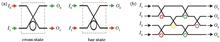
LONE: A Low-Loss, Non-Blocking, and Scalable 8-Port Optical Router
Jiaying Luo, Junyong Deng, Bowen Yang, Rui Shan, Ping Wang, and Chao Hui
The high bandwidth, low latency, and low power consumption of the on-chip optical interconnection can effectively alleviate the communication bottleneck of the electrical interconnection mode in a multicore processor. On-chip optical router is an essential part of the on-chip optical network design. With the gradual increase in processor scale, the traditional 4-port and 5-port can no longer meet the existing network density requirements. Additionally, with the expansion of the optical interconnection network, the problems such as communication congestion and low utilization of microring resonators have appeared. Therefore, this study proposes an 8-port on-chip optical router LONE to realize arbitrary communication between 8-port without blocking. OMNET++ simulation results show that LONE improves the utilization of microring resonators compared to optical routers of the same scale. Furthermore, the number of microring resonators is reduced by more than 41.67%, and insertion loss is reduced by more than 27.05%. The cost also has certain advantages, and the area overhead is reduced by more than 10%. Simultaneously, the biggest feature of the LONE structure is its simple structure, easy expansion, and adaptability to the needs of high-density networks. The high bandwidth, low latency, and low power consumption of the on-chip optical interconnection can effectively alleviate the communication bottleneck of the electrical interconnection mode in a multicore processor. On-chip optical router is an essential part of the on-chip optical network design. With the gradual increase in processor scale, the traditional 4-port and 5-port can no longer meet the existing network density requirements. Additionally, with the expansion of the optical interconnection network, the problems such as communication congestion and low utilization of microring resonators have appeared. Therefore, this study proposes an 8-port on-chip optical router LONE to realize arbitrary communication between 8-port without blocking. OMNET++ simulation results show that LONE improves the utilization of microring resonators compared to optical routers of the same scale. Furthermore, the number of microring resonators is reduced by more than 41.67%, and insertion loss is reduced by more than 27.05%. The cost also has certain advantages, and the area overhead is reduced by more than 10%. Simultaneously, the biggest feature of the LONE structure is its simple structure, easy expansion, and adaptability to the needs of high-density networks.
Laser & Optoelectronics Progress
- Publication Date: Feb. 10, 2022
- Vol. 59, Issue 3, 0313001 (2022)
Research on High-Efficiency Coupling Gratings Applied to Silicon Germanium Materials
Qiang Huang, Yi Zhang, Peilin Jiang, Changliang Yu, Haotian Shi, Chukun Huang, and Junqiang Sun
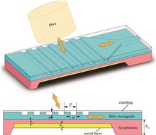
In this paper, we propose a SiGe grating coupler to realize vertical coupling between the single-mode fiber and the SiGe on-chip device. To improve the coupling efficiency of the SiGe grating, we adopted a metal layer as the reflecting mirror on the chip backside, and we optimized the structure, including the etch depth, etch groove width, and grating period, using the finite-different time-domain method. We computed the grating coupling efficiency by analyzing the power and electric field distribution with and without the metal reflective layer. The simulation results show that the maximum coupling efficiency of the uniform grating is increased by 9.4 dB compared with the case without a metal layer, and its directionality is significantly improved. The maximum coupling efficiency of the SiGe grating obtained by simulation optimization is -1.34 dB at 1466 nm. Furthermore, we simulated and designed a two-step apodized grating based on the uniform grating, which further increased the maximum coupling efficiency by 0.55 dB compared with the uniform. Additionally, we performed a tolerance analysis on the coupled grating, including the thickness of the metal layer, the refractive index of the SiGe material, and the size of the grating. The analysis results show that the SiGe grating has a high tolerance for process deviations. Also, we fabricated a SiGe coupling grating, and the test results show that the maximum coupling efficiency of -2.7 dB is obtained at 1465 nm. In this paper, we propose a SiGe grating coupler to realize vertical coupling between the single-mode fiber and the SiGe on-chip device. To improve the coupling efficiency of the SiGe grating, we adopted a metal layer as the reflecting mirror on the chip backside, and we optimized the structure, including the etch depth, etch groove width, and grating period, using the finite-different time-domain method. We computed the grating coupling efficiency by analyzing the power and electric field distribution with and without the metal reflective layer. The simulation results show that the maximum coupling efficiency of the uniform grating is increased by 9.4 dB compared with the case without a metal layer, and its directionality is significantly improved. The maximum coupling efficiency of the SiGe grating obtained by simulation optimization is -1.34 dB at 1466 nm. Furthermore, we simulated and designed a two-step apodized grating based on the uniform grating, which further increased the maximum coupling efficiency by 0.55 dB compared with the uniform. Additionally, we performed a tolerance analysis on the coupled grating, including the thickness of the metal layer, the refractive index of the SiGe material, and the size of the grating. The analysis results show that the SiGe grating has a high tolerance for process deviations. Also, we fabricated a SiGe coupling grating, and the test results show that the maximum coupling efficiency of -2.7 dB is obtained at 1465 nm.
Laser & Optoelectronics Progress
- Publication Date: Oct. 10, 2022
- Vol. 59, Issue 19, 1913002 (2022)
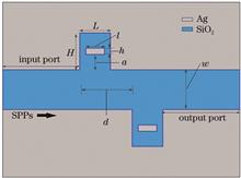
Design of Boundary Coupled Oblique Symmetric Double Rectangular Ring Metal-Insulator-Metal Structural Filter and Electro-Optic Switch
Mingyang Zhai, Guanmao Zhang, and Yunfei Yan
A metal-insulator-metal structural filter, which comprises two oblique symmetric rectangular ring resonant cavities and a waveguide, was built using a boundary coupling approach based on surface plasmon polaritons. A finite element method was employed to simulate and examine the filter, and the magnetic field distribution map and transmission curve were generated. The findings demonstrate that the filter’s maximum transmittance in the pass-band is 0.969, and its minimum transmittance in the stop-band is close to 0. This filter also has a wide pass-band and stop-band features, and a smooth transmission curve. The filter’s transmission curve can be red-shifted or blue-shifted by adjusting the structural parameters, and by setting certain structural parameters, the function of the on-off of the second and third communication windows of the filter can be controlled selectively while keeping the first communication window passing through. Thus, the filter can be employed as a band-pass/band-stop filter, which has crucial applications in high-density integrated circuits and optical fiber communication. furthermore, an electro-optic switch function can be accomplished by enhancing the structure and adding the electro-optic material DAST. A metal-insulator-metal structural filter, which comprises two oblique symmetric rectangular ring resonant cavities and a waveguide, was built using a boundary coupling approach based on surface plasmon polaritons. A finite element method was employed to simulate and examine the filter, and the magnetic field distribution map and transmission curve were generated. The findings demonstrate that the filter’s maximum transmittance in the pass-band is 0.969, and its minimum transmittance in the stop-band is close to 0. This filter also has a wide pass-band and stop-band features, and a smooth transmission curve. The filter’s transmission curve can be red-shifted or blue-shifted by adjusting the structural parameters, and by setting certain structural parameters, the function of the on-off of the second and third communication windows of the filter can be controlled selectively while keeping the first communication window passing through. Thus, the filter can be employed as a band-pass/band-stop filter, which has crucial applications in high-density integrated circuits and optical fiber communication. furthermore, an electro-optic switch function can be accomplished by enhancing the structure and adding the electro-optic material DAST.
Laser & Optoelectronics Progress
- Publication Date: Oct. 10, 2022
- Vol. 59, Issue 19, 1913001 (2022)
Broadband Linearization of Microwave Photonic Link Based on Single-Drive Dual-Parallel Mach-Zehnder Modulator
Huanjian Deng, Shangyuan Li, Shiming Yang, Qiang Liu, and Minming Geng
This study proposes a broadband linearization scheme based on a single-drive dual-parallel Mach-Zehnder modulator (SD-DPMZM) to improve the spurious-free dynamic range (SFDR) of microwave photonic link in broadband transmission. The third-order intermodulation distortion (IMD3) is theoretically eliminated using an 180° hybrid, thereby optimizing the biases of the dual-parallel Mach-Zehnder modulator. The simulated results show that IMD3 is completely suppressed when the input signal had two tones. An IMD3 suppression and SFDR improvement of 68 dB and 14.5 dB, respectively, are generated when SD-DPMZM is driven by two radio frequency tones of 10 and 10.01 GHz. Furthermore, results show that SFDR can remain above 114.3 dB·Hz2/3 when the signal is changed from the X-band to K-band. This study proposes a broadband linearization scheme based on a single-drive dual-parallel Mach-Zehnder modulator (SD-DPMZM) to improve the spurious-free dynamic range (SFDR) of microwave photonic link in broadband transmission. The third-order intermodulation distortion (IMD3) is theoretically eliminated using an 180° hybrid, thereby optimizing the biases of the dual-parallel Mach-Zehnder modulator. The simulated results show that IMD3 is completely suppressed when the input signal had two tones. An IMD3 suppression and SFDR improvement of 68 dB and 14.5 dB, respectively, are generated when SD-DPMZM is driven by two radio frequency tones of 10 and 10.01 GHz. Furthermore, results show that SFDR can remain above 114.3 dB·Hz2/3 when the signal is changed from the X-band to K-band.
Laser & Optoelectronics Progress
- Publication Date: Sep. 10, 2022
- Vol. 59, Issue 17, 1713002 (2022)

Design of New Type Light-Emitting Triode Device and Simulation Research on Photoelectric Regulation Performance
Jingjing Chen, Shaokun Hao, Xiongtu Zhou, Chaoxing Wu, Yongai Zhang, Tailiang Guo, and Jie Sun
Micro-light-emitting diodes (Micro-LEDs) offer many unique advantages in materials, devices, technologies, and process applications. In the future, display devices will evolve in the direction of multi-functional integration, such as lighting, swiching, and sensing, Micro-LEDs often require low-current-density driving, and the driving mode faces considerable challenges. To modulate LED devices with a low current input, herein, we propose a new type multifunctional integrated light-emitting triode device that integrates light emission and regulation functions, based on the same GaN material used in LEDs and process platform. The device shows a vertically integrated structure comprising bipolar transistors and LEDs. The number of electrons moving to the light-emitting active layer can be controlled by changing the base voltage, and the luminous effect of the device is simultaneously adjusted. Based on the current gain effect of bipolar junction transistor (BJT), the input current under the same light effect can be reduced from the milliampere to the microampere level and a highly linear regulation is achieved within a certain voltage range. The device can be controlled and driven using low-power signals and is expected to become a revolutionary technology for high-density and high-integration smart displays. Micro-light-emitting diodes (Micro-LEDs) offer many unique advantages in materials, devices, technologies, and process applications. In the future, display devices will evolve in the direction of multi-functional integration, such as lighting, swiching, and sensing, Micro-LEDs often require low-current-density driving, and the driving mode faces considerable challenges. To modulate LED devices with a low current input, herein, we propose a new type multifunctional integrated light-emitting triode device that integrates light emission and regulation functions, based on the same GaN material used in LEDs and process platform. The device shows a vertically integrated structure comprising bipolar transistors and LEDs. The number of electrons moving to the light-emitting active layer can be controlled by changing the base voltage, and the luminous effect of the device is simultaneously adjusted. Based on the current gain effect of bipolar junction transistor (BJT), the input current under the same light effect can be reduced from the milliampere to the microampere level and a highly linear regulation is achieved within a certain voltage range. The device can be controlled and driven using low-power signals and is expected to become a revolutionary technology for high-density and high-integration smart displays.
Laser & Optoelectronics Progress
- Publication Date: Sep. 10, 2022
- Vol. 59, Issue 17, 1713001 (2022)
Application of Silicon-Based Microring Resonant Cavity in Integrated Optical Gyroscope Sensitive Unit
Daoxin Sun, Dongliang Zhang, Fu Bi, Lidan Lu, Zhehai Zhou, and Lianqing Zhu
As an optically sensitive unit, the silicon-based integrated photonic resonator plays a vital role in the performance of chip-scale optical gyroscopes. In this paper, the integrated resonator of the photonic integrated gyroscope with the enhanced reciprocity-sensitive dual micro-ring architecture is the research object. The key structural parameters of the dual microring resonator are analyzed through finite-difference time-domain simulation. Constructing a simulation link allowed the study on the internal relationships between quality factor, fineness, coupling coefficient, and transmission loss. The resulting insights formed the basis for structural layout design. The dual microring resonant cavity device is then fabricated through a multiproject wafer tape-out using a passive silicon-based photonic integration process. Test results show that, for a microring radius of 500 μm, the coupling coefficient between waveguide and microring is 0.3, the working wavelength is around 1550 nm, the free spectral range is 0.182 nm, the 3 dB bandwidth is 0.045 nm, the fineness is 4.04, and the quality factor is ~3.4×10⁴. These research results provide a firm foundation for further design optimization of the dual microring resonator. As an optically sensitive unit, the silicon-based integrated photonic resonator plays a vital role in the performance of chip-scale optical gyroscopes. In this paper, the integrated resonator of the photonic integrated gyroscope with the enhanced reciprocity-sensitive dual micro-ring architecture is the research object. The key structural parameters of the dual microring resonator are analyzed through finite-difference time-domain simulation. Constructing a simulation link allowed the study on the internal relationships between quality factor, fineness, coupling coefficient, and transmission loss. The resulting insights formed the basis for structural layout design. The dual microring resonant cavity device is then fabricated through a multiproject wafer tape-out using a passive silicon-based photonic integration process. Test results show that, for a microring radius of 500 μm, the coupling coefficient between waveguide and microring is 0.3, the working wavelength is around 1550 nm, the free spectral range is 0.182 nm, the 3 dB bandwidth is 0.045 nm, the fineness is 4.04, and the quality factor is ~3.4×10⁴. These research results provide a firm foundation for further design optimization of the dual microring resonator.
Laser & Optoelectronics Progress
- Publication Date: Jul. 10, 2022
- Vol. 59, Issue 13, 1313001 (2022)
Reverse Design of Photonic Devices Based on a Hybrid Particle Swarm Algorithm
Yinghan Li, Lü Jie, Lin Jiang, and Linghao Cheng
Particle swarm optimization (PSO) algorithm has good global optimization ability . However, PSO has some disadvantages such as the tendency to easily fall into local extremes, slow convergence speed, and low convergence accuracy at the late stage of the algorithm. Therefore, this study optimizes the traditional PSO algorithm, affording a simplified version and introducing random disturbances to facilitate the falling out of local extremes, thus enhancing its performance on global optimization. Moreover, a hybrid algorithm for the inverse design of photonic devices is proposed by combining PSO and the greedy algorithm with the gradient descent method to evaluate automatic switching between algorithms. Compared with the traditional PSO algorithm, the proposed hybrid algorithm shows better performance on global optimization with a faster convergence speed, higher accuracy, and superior design efficiency. A 1∶1 optical splitter is inversely designed using the proposed hybrid algorithm. At a bandwidth of 120 nm, the range of insertion loss at the output of the device is 0.125 dB?0.197 dB. Moreover, the device is manufacturable robustness. Particle swarm optimization (PSO) algorithm has good global optimization ability . However, PSO has some disadvantages such as the tendency to easily fall into local extremes, slow convergence speed, and low convergence accuracy at the late stage of the algorithm. Therefore, this study optimizes the traditional PSO algorithm, affording a simplified version and introducing random disturbances to facilitate the falling out of local extremes, thus enhancing its performance on global optimization. Moreover, a hybrid algorithm for the inverse design of photonic devices is proposed by combining PSO and the greedy algorithm with the gradient descent method to evaluate automatic switching between algorithms. Compared with the traditional PSO algorithm, the proposed hybrid algorithm shows better performance on global optimization with a faster convergence speed, higher accuracy, and superior design efficiency. A 1∶1 optical splitter is inversely designed using the proposed hybrid algorithm. At a bandwidth of 120 nm, the range of insertion loss at the output of the device is 0.125 dB?0.197 dB. Moreover, the device is manufacturable robustness.
Laser & Optoelectronics Progress
- Publication Date: Jun. 10, 2022
- Vol. 59, Issue 11, 1113001 (2022)
Registration Method of Video Image and Laser Point Cloud Under Moving Measurement
Lujiu Zha, Yonghua Xia, Bin Wang, Minglong Yang, Yirong Pan, Ruo Chen, and Qi Zhu
Motion measurement system can simultaneously collect three-dimensional (3D) laser point clouds, image texture, and the position and attitude data; however the registration fusion of image photos and laser point cloud is challenging to meet the needs of high efficiency and high overlap. This paper proposes a method to register video images with laser point clouds under motion measurement to solve this problem. The positioning orientation system (POS) sensor’s position and attitude data are used to calculate the initial registration value of keyframes in a video image and a laser point cloud using a collinear equation model. The iterative method for selecting weights based on Robust estimation improves the accuracy of initial registration values and determines the exact values of registration parameters. The stereo-dense matching point cloud is generated from the keyframe of the video image, and the nearest neighbor iterative registration is performed using the 3D laser point cloud. The experimental results show that the registration method of video image and a vehicular laser point cloud is feasible, and the registration accuracy is high, meeting the requirements of 3D reconstruction of urban streets, component acquisition, target extraction, and other measurement applications. Motion measurement system can simultaneously collect three-dimensional (3D) laser point clouds, image texture, and the position and attitude data; however the registration fusion of image photos and laser point cloud is challenging to meet the needs of high efficiency and high overlap. This paper proposes a method to register video images with laser point clouds under motion measurement to solve this problem. The positioning orientation system (POS) sensor’s position and attitude data are used to calculate the initial registration value of keyframes in a video image and a laser point cloud using a collinear equation model. The iterative method for selecting weights based on Robust estimation improves the accuracy of initial registration values and determines the exact values of registration parameters. The stereo-dense matching point cloud is generated from the keyframe of the video image, and the nearest neighbor iterative registration is performed using the 3D laser point cloud. The experimental results show that the registration method of video image and a vehicular laser point cloud is feasible, and the registration accuracy is high, meeting the requirements of 3D reconstruction of urban streets, component acquisition, target extraction, and other measurement applications.
Laser & Optoelectronics Progress
- Publication Date: May. 25, 2022
- Vol. 59, Issue 10, 1013001 (2022)
Wide Optical Frequency Comb System Based on Single Intensity Modulator
Junping Gao, Mengmeng Zhao, Jia Lu, Jianfei Liu, and Jingfei He
This paper proposes a scheme which uses a single Mach-Zehnder modulator (MZM) to generate a flat and wide optical comb based on the double-sideband modulation method. The frequency difference between two lasers directly determines the spectral width and quality of this comb after double-sideband modulation. Through the theoretical analysis of the standard deviation between the sidebands of different orders under different modulation coefficients and the Bessel value of each order sideband, we find sidebands above the fifth order have a negligible effect on the wide comb. The lower-power fifth-order sidebands are superimposed on the sidebands of different orders, so that the powers of the sidebands of different orders can be compensated or cancelled, thereby reducing the influence of the higher-order sidebands on the optical frequency comb and improving the flatness. The flatness of the wide optical comb obtained by simulation reaches 3.7 dB, and the effective spectral width is 700 GHz. After the non-return to zero data with transmission rate of 5 Gbit·s-1 is modulated on this optical comb and transmitted through an optical fiber, the eye diagram is still clearly visible, and the power penalty is less than 1.8 dB at the bit error rate level of 10-9. Such an optical comb can transmit more data information in optical communications, realize high-speed data transmission and maintain the flatness of the optical comb with good stability and low cost. This paper proposes a scheme which uses a single Mach-Zehnder modulator (MZM) to generate a flat and wide optical comb based on the double-sideband modulation method. The frequency difference between two lasers directly determines the spectral width and quality of this comb after double-sideband modulation. Through the theoretical analysis of the standard deviation between the sidebands of different orders under different modulation coefficients and the Bessel value of each order sideband, we find sidebands above the fifth order have a negligible effect on the wide comb. The lower-power fifth-order sidebands are superimposed on the sidebands of different orders, so that the powers of the sidebands of different orders can be compensated or cancelled, thereby reducing the influence of the higher-order sidebands on the optical frequency comb and improving the flatness. The flatness of the wide optical comb obtained by simulation reaches 3.7 dB, and the effective spectral width is 700 GHz. After the non-return to zero data with transmission rate of 5 Gbit·s-1 is modulated on this optical comb and transmitted through an optical fiber, the eye diagram is still clearly visible, and the power penalty is less than 1.8 dB at the bit error rate level of 10-9. Such an optical comb can transmit more data information in optical communications, realize high-speed data transmission and maintain the flatness of the optical comb with good stability and low cost.
Laser & Optoelectronics Progress
- Publication Date: Jan. 01, 2021
- Vol. 58, Issue 9, 0913001 (2021)
Topics
© Copyright 2018-2021 | Chinese Laser Press. All Rights Reserved 沪ICP备15018463号-20